1. An RF power amplifier, comprising:
a first field effect transistor:
having a first gate, a first source, and a first drain,
having an output power rating of at least 200 watts, and
operating with a drain-to-source voltage that is greater than 50 VDC;
a second field effect transistor:
having a second gate, a second source, and a second drain,
having an output power rating of at least 200 watts, and
operating with a drain-to-source voltage that is greater than 50 VDC;
wherein said transistors are configured as a push-pull amplifier;
an RF signal input;
an input transformer connected to the RF signal input, the input transformer having respective balanced outputs connected to the first gate and the second gate;
a broadband output transformer having a first balanced input connected to the first drain, and a second balanced input connected to the second drain, wherein the broadband output transformer has an input to output impedance ratio of 1:4, and further wherein at least some flux cancellation occurs within the broadband output transformer; and
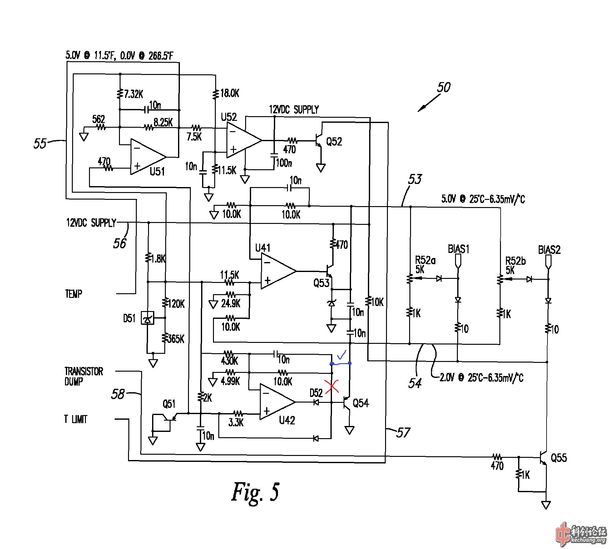
temperature compensating bias circuitry for providing a temperature compensated bias voltage to the first field effect transistor and the second field effect transistor for decreasing the bias voltage of the first field effect transistor and the second field effect transistor as transistor temperature increases, the temperature compensating bias circuitry comprising:
a temperature sensor generating a temperature signal;
a first amplifier having an output providing a first temperature dependent voltage based on the temperature signal;
a second amplifier having an output providing a second temperature dependent voltage based on the temperature signal, wherein the first temperature dependent voltage and the second temperature dependent voltage change at substantially the same rate in response to the temperature signal; and
a potentiometer connected to the output of the first amplifier and the output of the second amplifier such that a voltage across the potentiometer remains substantially constant when the first temperature dependent voltage and the second temperature dependent voltage change; and
a bias output connected to at least one of the first field effect transistor and the second field effect transistor and supplying the temperature compensated bias voltage to the at least one of the first field effect transistor and the second field effect transistor.
2. A modular RF power amplifier system, comprising:
a first amplifier module comprising the RF power amplifier as set forth in claim 1; and
a second amplifier module comprising the RF power amplifier as set forth in claim 1;
wherein outputs from said modules are combined to form a combined RF output.
3. The RF power amplifier of claim 1, further comprising:
an RF output terminal;
an output balun transformer; and
a DC-blocking capacitor, wherein the output balun transformer and the DC-blocking capacitor are connected in series between the broadband output transformer and the RF output terminal,
wherein the broadband output transformer is a transmission line transformer including a cable having a characteristic impedance of approximately or exactly 25 ohms,
wherein the broadband output transformer has balanced outputs and during operation of the RF power amplifier a net flux within the broadband output transformer is substantially zero, and
wherein the output balun transformer has an input to output impedance ratio of 1:1 and a characteristic impedance of approximately or exactly 50 ohms.
4. An RF power amplifier, comprising:
a first plurality of field effect transistors having directly interconnected drains and respective output power ratings of at least 100 watts;
a second plurality of field effect transistors having directly interconnected drains and respective output power ratings of at least 100 watts;
wherein said transistors operate with a drain-to-source voltage that is greater than 50 VDC, and
wherein the first plurality of field effect transistors and the second plurality of field effect transistors together form a push-pull amplifier having an output power rating of at least 400 watts;
an RF signal input;
an input transformer connected to the RF signal input, the input transformer having respective balanced outputs connected to gates of the first plurality of field effect transistors and gates of the second plurality of field effect transistors; and
a broadband output transformer having a first balanced input connected to the drains of the first plurality of field effect transistors, and a second balanced input connected to the drains of the second plurality of field effect transistors, wherein the broadband output transformer has an input to output impedance ratio of 1:4, and further wherein at least some flux cancellation occurs within the broadband output transformer; and
temperature compensating bias circuitry for providing a temperature compensated bias voltage to the first plurality of field effect transistors and the second plurality of field effect transistors for decreasing the bias voltage of the first plurality of field effect transistors and the second plurality of field effect transistors as transistor temperature increases, the temperature compensating bias circuitry comprising:
a temperature sensor generating a temperature signal;
a first amplifier having an output providing a first temperature dependent voltage based on the temperature signal;
a second amplifier having an output providing a second temperature dependent voltage based on the temperature signal, wherein the first temperature dependent voltage and the second temperature dependent voltage change at substantially the same rate in response to the temperature signal; and
a potentiometer connected to the output of the first amplifier and the output of the second amplifier such that a voltage across the potentiometer remains substantially constant when the first temperature dependent voltage and the second temperature dependent voltage change; and
a bias output connected to at least one of the first plurality of field effect transistors and the second plurality of field effect transistors and supplying the temperature compensated bias voltage to the at least one of the first plurality of field effect transistors and the second plurality of field effect transistors.
5. A modular RF power amplifier system, comprising:
a first amplifier module comprising the RF power amplifier as set forth in claim 4; and
a second amplifier module comprising the RF power amplifier as set forth in claim 4, wherein outputs from said modules are combined to form a combined RF output.
6. The RF power amplifier of claim 4, further comprising:
an RF output terminal;
an output balun transformer; and
a DC-blocking capacitor, wherein the output balun transformer and the DC-blocking capacitor are connected in series between the broadband output transformer and the RF output terminal,
wherein the broadband output transformer is a transmission line transformer including a cable having a characteristic impedance of approximately or exactly 25 ohms,
wherein the broadband output transformer has balanced outputs and during operation of the RF power amplifier a net flux within the broadband output transformer is substantially zero, and
wherein the output balun transformer has an input to output impedance ratio of 1:1 and a characteristic impedance of approximately or exactly 50 ohms.
7. An RF power amplifier, comprising:
a push-pull amplifier, the push-pull amplifier comprising a first field effect transistor and a second field effect transistor; and
temperature compensating bias circuitry for providing a temperature compensated bias voltage to the first field effect transistor and the second field effect transistor for decreasing the bias voltage of the first field effect transistor and the second field effect transistor as transistor temperature increases, the temperature compensating bias circuitry comprising:
a temperature sensor generating a temperature signal;
a first amplifier having an output providing a first temperature dependent voltage based on the temperature signal; and
a potentiometer connected to the output of the first amplifier such that a voltage across the potentiometer remains substantially constant when the first temperature dependent voltage changes; and
a bias output connected to at least one of the first field effect transistor and the second field effect transistor and supplying the temperature compensated bias voltage to the at least one of the first field effect transistor and the second field effect transistor.
8. The RF power amplifier of claim 7, wherein the temperature compensating bias circuitry further comprises a second amplifier having an output providing a second temperature dependent voltage based on the temperature signal,
wherein the first temperature dependent voltage and the second temperature dependent voltage change at substantially the same rate in response to the temperature signal, and
wherein the potentiometer is connected to the output of the first amplifier and the output of the second amplifier such that a voltage across the potentiometer remains substantially constant when the first temperature dependent voltage and the second temperature dependent voltage change.
9. The RF power amplifier of claim 8, further comprising a follower transistor connected to the potentiometer, wherein the follower transistor generates the bias output.
10. The RF power amplifier of claim 7, wherein the temperature sensor is a transistor.
11. The RF power amplifier of claim 7, wherein the temperature sensor comprises a temperature sensor integrated circuit.
12. The RF power amplifier of claim 7, further comprising a temperature output signal transmitting a temperature of the RF power amplifier.
13. The RF power amplifier of claim 7, further comprising a transistor dump signal for deactivating at least one of the first field effect transistor and the second field effect transistor.
14. The RF power amplifier of claim 7, wherein the first field effect transistor includes a first gate, a first source, and a first drain,
wherein the second field effect transistor includes a second gate, a second source, and a second drain, the RF power amplifier further comprising:
a broadband output transformer having a first balanced input and a second balanced input, wherein the broadband output transformer has an input to output impedance ratio of 1:4, and further wherein at least some flux cancellation occurs within the broadband output transformer;
a first DC-blocking transformer connected between the first balanced input and the first drain; and
a second DC-blocking transformer connected between the second balanced input and the second drain.
15. The RF power amplifier of claim 14, wherein each one of the broadband output transformer, the first DC-blocking transformer, and the second DC-blocking transformer include a cable having a characteristic impedance of approximately or exactly 25 ohms.
16. The RF power amplifier of claim 14, wherein the first DC-blocking transformer provides a negative feedback signal to the first field effect transistor, and wherein the second DC-blocking transformer provides a negative feedback signal to the second field effect transistor.
17. The RF power amplifier of claim 14, further comprising another transformer, which provides negative feedback signals to the first field effect transistor and the second field effect transistor.
18. The RF power amplifier of claim 14, further comprising
an RF output terminal; and
an output balun transformer connected between the broadband output transformer and the RF output terminal.
19. An RF power amplifier, comprising:
a push-pull amplifier, the push-pull amplifier comprising a first field effect transistor having a first drain and a second field effect transistor having a second drain;
a broadband output transformer having a first balanced input and a second balanced input;
a first DC-blocking transformer connected between the first balanced input and the first drain; and
a second DC-blocking transformer connected between the second balanced input and the second drain.
20. The RF power amplifier of claim 19, further comprising temperature compensating bias circuitry for providing a temperature compensated bias voltage to the first field effect transistor and the second field effect transistor for decreasing the bias voltage of the first field effect transistor and the second field effect transistor as transistor temperature increases.
21. The RF power amplifier of claim 19, wherein each one of the broadband output transformer, the first DC-blocking transformer, and the second DC-blocking transformer include a cable having a characteristic impedance of approximately or exactly 25 ohms.
22. The RF power amplifier of claim 19, wherein the first DC-blocking transformer provides a negative feedback signal to the first field effect transistor, and wherein the second DC-blocking transformer provides a negative feedback signal to the second field effect transistor.
23. The RF power amplifier of claim 19, further comprising another transformer, which provides negative feedback signals to the first field effect transistor and the second field effect transistor.
24. The RF power amplifier of claim 19, wherein the broadband output transformer has an input to output impedance ratio of 1:4, and further wherein at least some flux cancellation occurs within the broadband output transformer.
25. The RF power amplifier of claim 24, further comprising
an RF output terminal; and
an output balun transformer connected between the broadband output transformer and the RF output terminal.
26. The RF power amplifier of claim 19, wherein the broadband output transformer has unbalanced outputs and an input to output impedance ratio of 1:1.
27. The RF power amplifier of claim 26, further comprising
an RF output terminal; and
an unbalanced-to-unbalanced transformer connected between the broadband output transformer and the RF output terminal.
28. The RF power amplifier of claim 27, wherein the unbalanced-to-unbalanced transformer has an input to output impedance ratio of 1:4.
29. An RF power amplifier, comprising:
a first amplifier module comprising a first push-pull amplifier including a plurality of field effect transistors and a first output balun transformer, wherein an output impedance of the first amplifier module is 25 ohms;
a second amplifier module comprising a second push-pull amplifier including a plurality of field effect transistors and a second output balun transformer, wherein an output impedance of the second amplifier module is 25 ohms;
a combiner connected to the first amplifier module and the second amplifier module, the combiner comprising an unbalanced-to-unbalanced output transformer having an input-to-output impedance ratio of 1:4,
wherein the combiner combines an output from the first amplifier module and an output from the second amplifier module into a combined signal,
wherein the combined signal is supplied to the unbalanced-to-unbalanced output transformer, and
wherein an output impedance of the combiner is 50 ohms.
30. The RF power amplifier of claim 29, wherein the first amplifier module includes a plurality of DC-blocking transformers, and wherein the second amplifier module includes a plurality of DC-blocking transformers.


200字以内,仅用于支线交流,主线讨论请采用回复功能。